A Fiber Array Unit (FAU) is a passive optical assembly: it positions multiple optical fibers at a fixed pitch with high precision and bonds them to the edge of a photonic integrated circuit (PIC). It is the standard interface for edge coupling between the fiber world and the chip world. A typical FAU consists of a V-groove substrate, a fiber array, a lid, and optical adhesive[1][2].
The FAU matters because the coupling loss at the FAU–chip interface goes directly into the optical budget of the whole transceiver, and its long-term drift determines module reliability. In 800G and CPO (co-packaged optics) architectures, the channel count keeps growing, and the FAU’s error sources scale with the channel count[1].
The answer: the errors come from three layers — manufacturing tolerances (V-groove pitch, core/cladding concentricity, end-face angle), assembly misalignment (lateral, angular, axial gap, mode-field-diameter mismatch), and long-term drift (thermal expansion mismatch, adhesive stress, wavelength dependence). This article first explains the FAU structure, then derives the coupling loss for each misalignment, and finally summarizes the error sources with their typical magnitudes.
1. The problem: where the FAU sits in the optical path
The signal path in a high-speed optical interconnect is: fiber → FAU → PIC → electrical interface → chip[1]. The FAU performs no optical function itself; it only aligns the fiber array precisely and bonds it stably to the chip-side optical interface[1].
There are two coupling architectures:
- Edge coupling: the fiber end faces are directly aligned with the waveguide facets at the chip edge, and light travels horizontally into the chip waveguide. Advantages: direct optical path, high coupling efficiency, broad bandwidth[1]. The FAU is the standard component for edge coupling.
- Grating coupling: light is redirected by a 45° mirror and a microlens, then enters a grating coupler on the chip surface vertically. Advantages: compatibility with 2D fiber arrays and convenient wafer-level testing[1].
Terminology: an FA (Fiber Array) is the fiber array itself; an FAU is the complete assembly after precision alignment, fixation, and packaging[1].
Key FAU parameters: channel count and fiber type, pitch (standard 127 µm and 250 µm), core positioning accuracy, end-face angle, polarization handling (PM fiber slow-axis orientation), package form[2][3].
2. The structure: V-groove, fiber array, lid, adhesive
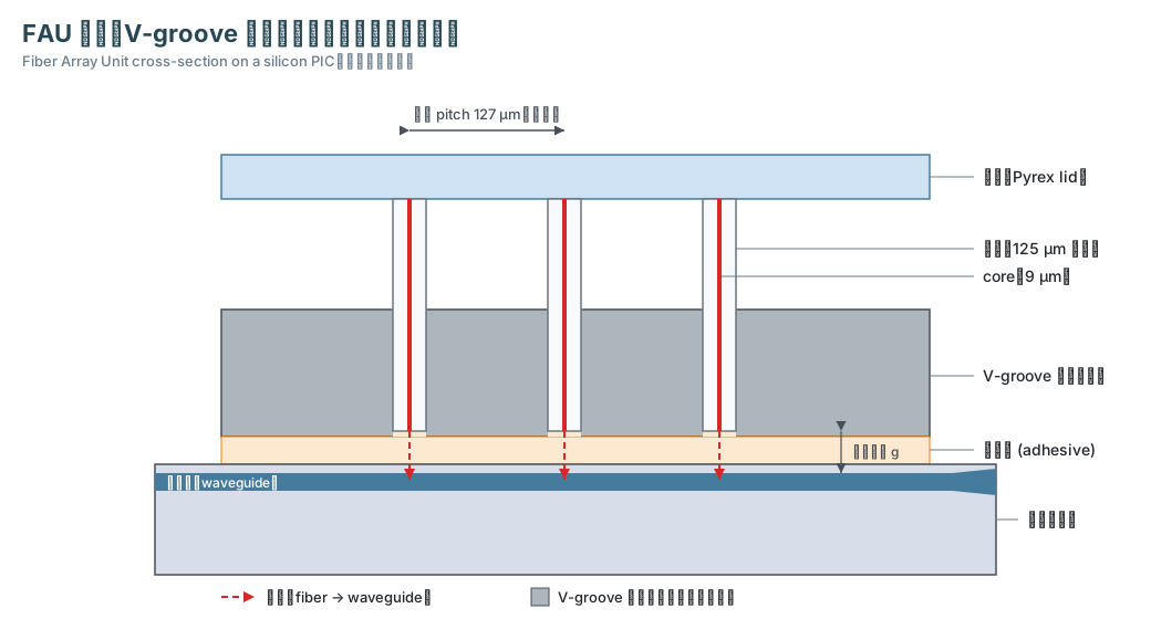
Figure 1: FAU cross-section (schematic, not to scale). The V-grooves run through the substrate, the fiber axes are perpendicular to the chip, and the end faces sit at the adhesive–chip interface. The V-grooves constrain the fibers laterally, keeping pitch and height consistent across channels.
The four FAU components (top to bottom):
- Lid: holds the fiber array in place. OZ Optics uses an optically clear Pyrex lid, which allows UV-curable adhesive for fast bonding[2].
- Fiber array: single-mode (SMF-28, 9/125 µm), multimode (50/125 or 62.5/125 µm), or polarization-maintaining (PANDA, 8/125 µm) fibers, in ribbon or individual form[2]. During assembly, the coating is stripped over the designated section and the bare fiber is placed in the V-groove[1].
- V-groove substrate: a silicon, fused-silica, or ceramic substrate; the V-grooves are made by precision machining and set the position, pitch, and height of each fiber[1][3]. OZ Optics’ pitch accuracy standard is ±0.5 µm (absolute)[2].
- Optical adhesive: UV- or heat-curable, bonding the FAU to the chip. The adhesive is in the optical path and must transmit the operating wavelength[2].
Manufacturing flow: precision V-groove machining → fiber placement → core position measurement → active alignment → bonding[1][2]. Core position measurement uses white-light illumination plus automated video measurement: the fibers are illuminated, the centers of the first and last illuminated fibers define a reference centerline, and each core’s deviation from its ideal position is measured[2]. Bonding uses a 3- or 6-axis micro-stage for active alignment, optimizing the coupling of the first and last fibers of the array, then adhesive is applied[2].
Key specs (OZ Optics standard products):
| Parameter | Value |
|---|---|
| Channel count | 1–96 (standard 2–48) |
| Pitch | 127 µm, 250 µm (custom 400, 500 µm) |
| V-groove pitch accuracy | ±0.5 µm (absolute) |
| Insertion loss | <0.5 dB per fiber |
| End-face angle | 0° or 8° ± 0.3° (8° reduces back-reflection) |
| Return loss | <40 dB (PC), <50 dB (Ultra), <60 dB (APC) |
3. The principle: where the coupling errors come from
The coupling efficiency between fiber and waveguide is the overlap integral of the two mode fields. Under the Gaussian approximation, each of the four misalignments has a closed-form loss expression[4]. Computed for a single-mode fiber at 1310 nm (mode field radius w₀ = 4.65 µm, i.e., MFD ≈ 9.3 µm):
Lateral misalignment (offset d):
η = exp(−d²/w₀²)
d = 1 µm → 4.5% loss (0.20 dB); d = 2 µm → 16.9% (0.80 dB) (computed from the formula).
Angular misalignment (end-face tilt θ):
η = exp(−(π w₀ θ/λ)²)
θ = 1° → 3.8% (0.17 dB); θ = 2° → 14.3% (0.67 dB) (computed from the formula).
Axial gap (end-face separation g):
η = 1/(1 + (λg/(π w₀²))²)
Rayleigh range zR = πw₀²/λ ≈ 52 µm. g = 10 µm → 3.5% (0.16 dB); g = 20 µm → 12.8% (0.59 dB); g = 50 µm → 47.8% (2.82 dB) (computed from the formula).
Mode-field-diameter mismatch (MFD mismatch):
η = (2w₁w₂/(w₁²+w₂²))²
20% mismatch → 3.3% (0.14 dB) (computed from the formula).
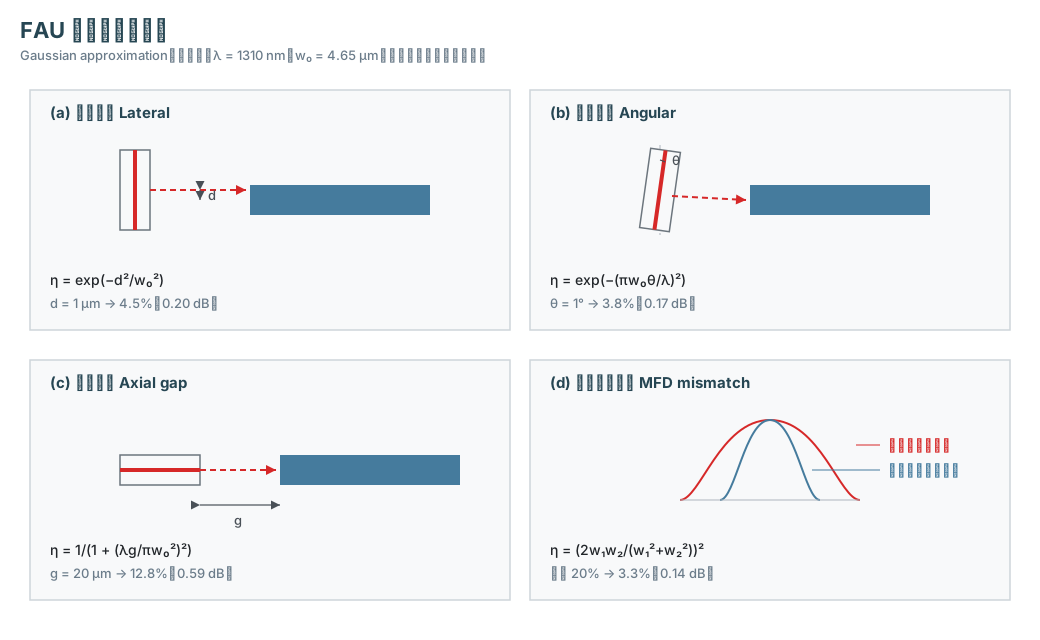
Figure 2: Schematics of the four coupling misalignments with the Gaussian-approximation loss formulas. Computed examples use λ = 1310 nm, w₀ = 4.65 µm (schematic; values computed from the formulas).
These errors have two properties[4]:
- Non-linear: the loss grows quadratically with the misalignment, so small-misalignment results cannot be extrapolated linearly.
- Correlated: an end-face tilt produces both angular loss and a lateral offset (larger farther from the end face). The correct combination is to convert each loss to a transmission factor and multiply, or take the RSS (root-sum-square) in dB.
The Moore tutorial’s tolerancing example: to keep the total coupling loss under 0.46 dB (10%), the lateral, angular, and axial misalignments must each be controlled to a loss contribution of about 0.2–0.3 dB, and the mode-field mismatch to about 0.04 dB; the RSS total is 0.45 dB[4].
Mapped to FAU error sources:
| Misalignment | FAU error source | Typical magnitude (source) |
|---|---|---|
| Lateral | V-groove machining tolerance (±0.5 µm, OZ Optics spec) + core/cladding concentricity (SMF-28 <0.5 µm) | total <1 µm[2] |
| Angular | End-face angle tolerance (8° ± 0.3° is the design value); residual tilt after active alignment | not given in sources |
| Axial | Bonding gap (adhesive thickness and end-face contact) | not given in sources |
| Mode field | Fiber MFD vs chip waveguide mode; the silicon waveguide mode is smaller than the fiber, so a mode size converter (tapered waveguide) is often needed[3] | not given in sources |
4. Limitations: long-term drift and what cannot be controlled
Manufacturing and assembly errors are fixed at the factory; long-term drift comes from the environment:
- Thermal expansion mismatch: silicon, silica fiber, and adhesive have different coefficients of thermal expansion (CTE). Temperature changes deform the FAU and the chip by different amounts, producing thermomechanical misalignment. Silicon, silicon dioxide, and glass substrates match Si-based PICs well in CTE; in high-channel-count CPO packages, the thermally induced warpage between the FAU and the edge coupler array must be specifically evaluated in the package design[5]. The adhesive’s CTE is a key factor for long-term reliability[6].
- Adhesive: the adhesive is in the optical path (it must transmit the operating wavelength[2]), and its curing shrinkage and stress cause performance drift[6].
- Wavelength dependence: the fiber mode field diameter changes with wavelength, so the coupling loss varies with wavelength. The FAU insertion-loss spec is given at a specific wavelength[2][3].
- Polarization: the PM fiber slow axis must be aligned to the chip’s polarization direction, otherwise polarization-dependent loss (PDL) appears. OZ Optics’ PM array assemblies specify an extinction ratio up to 30 dB[2].
- Test uncertainty: in wafer-level PIC testing, the FAU, the micro-stage, and the light source are the main sources of test variation; the same die can cross a pass/fail threshold because of FAU coupling variation[7].
5. The answer: error sources summarized
| Error source | Layer | Typical magnitude / spec (source) | Impact |
|---|---|---|---|
| V-groove machining tolerance (pitch) | Manufacturing | ±0.5 µm (absolute, OZ Optics spec)[2] | Lateral misalignment, channel-to-channel consistency |
| Fiber core/cladding concentricity | Manufacturing (fiber) | <0.5 µm (SMF-28)[2] | Lateral misalignment |
| End-face angle | Manufacturing | 8° ± 0.3° (design value)[2] | Angular misalignment, return loss |
| Bonding gap | Assembly | not given in sources | Axial loss |
| Residual tilt after active alignment | Assembly | not given in sources | Angular + lateral |
| Mode-field mismatch | Design | silicon waveguide mode smaller than fiber; mode size converter often needed[3] | Intrinsic loss |
| Thermal expansion mismatch | Environment | Si/SiO₂/glass substrates CTE-match the Si chip[5] | Long-term drift, warpage |
| Adhesive CTE and stress | Environment | key factor for long-term reliability[6] | Long-term drift |
| Wavelength dependence | Environment | mode field changes with wavelength[2][3] | coupling loss varies with wavelength |
| PM axis misalignment | Manufacturing/assembly | assembly ER up to 30 dB[2] | Polarization-dependent loss |
Common misconceptions
- “The FAU is a passive component, so it doesn’t affect the system”: wrong. The FAU’s coupling loss goes directly into the optical budget, its long-term drift determines module reliability, and in wafer-level testing the FAU is a main source of test uncertainty[7].
- “Lower insertion loss means a better FAU”: wrong. Return loss (end-face angle), polarization-dependent loss, and long-term drift matter just as much; the 8° end-face angle is a trade-off between return loss and coupling loss[2].
- “127 µm pitch is universal”: wrong. Standard pitches are 127 and 250 µm, with 400/500 µm and custom pitches also available; the pitch is set by the chip waveguide design[2].
Self-check for readers
- What are the four FAU components, and what is each one responsible for?
- Why can’t the lateral and angular misalignment losses simply be added?
- Why must high-channel-count CPO packages specifically evaluate the FAU’s thermally induced warpage?
Back to the opening question: where do the FAU’s coupling errors come from? From three layers: manufacturing tolerances (V-groove ±0.5 µm, core concentricity <0.5 µm, end-face angle ±0.3°), assembly misalignment (lateral, angular, axial gap, mode-field mismatch — 1 µm lateral or 1° angular is already about 0.2 dB), and long-term drift (thermal expansion mismatch, adhesive stress, wavelength dependence). The Gaussian approximation gives a closed-form loss formula for each misalignment, and the tolerancing method is to keep each error’s loss contribution to about 0.2–0.3 dB.
Applicable conditions and limits: the formulas here are the Gaussian approximation for single-mode edge coupling, and the computed examples use 1310 nm, w₀ = 4.65 µm; the 1550 nm fiber mode field is larger, and the numbers must be recomputed. The error sources of grating coupling, CTE values of specific materials, and the residual tilt and axial gap of specific assembly processes are not covered by the sources cited here.